HD-KFM(KPFM) developed by CSI for the Nano-Observer AFM has the advantage of amplifying the feedback signal through the second eigenmode of the cantilever. Also it allows a much closer probe of the electric field created by the surface potential compared to other approaches. This is of extreme relevance when imaging small molecules or bidimensional materials.
Surface potential mapping
2nd lock-in amplifier
NO LIFT : Very high sensitivity & higher spatial resolution
Applications
Materials science
Semiconductor
Polymer
Life science
產品介紹
表面電位檢測")
KPFM(HD-KFM)表面電位檢測
概觀
HD-KFM : THE MOST ADVANCED SINGLE-PASS KFM MODE
On the contrary to standard single-pass setups, Bimodal HD-KFM is characterized because the electric feedback is tuned to the second eigenmode frequency of the cantilever. Figure 1 shows the concept on which HD-KFM is based: the first flexural eigenmode of the cantilever is excited mechanically and the second flexural mode is excited electrically. In the past decade, multi-frequency approach has become one of the front-end topics amongst the AFM community as it has shown many potential applications.
The advantages of tuning the VAC bias used for the electric feedback to the second eigenmode of the cantilever is that the signal is amplified by the Q factor of the second eigenmode. This effect provides the possibility to use smaller VAC values to obtain an oscillation amplitude with an acceptable signal to noise ratio as compared to other implementations not-based on the second eigenmode amplification. Additionally, stiffer effective spring constant of the second eigenmode provides more stability of the oscillation during the scanning of the surface. In Figure 2, it is shown an schematics of the HD-KFM setup implementation with the electric diagram of HDKFM where the first flexural mode is excited mechanically and the second flexural mode is excited electrically. The topographic feedback operates on the mechanical amplitude (lock-in 1) and the electrical feedback operates on the electric amplitude (lock-in 2).
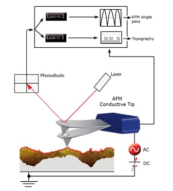
Figure 1 : schematics of Bimodal HD-KFM setup
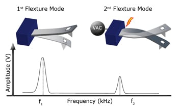
Figure 2 : Concept of Bimodal HD-KFM: firtst flexural mode (or eigenmode) frequency is excited mechanically to measure topography, while the second flexural mode frequency is excited electrically to measure surface potential.
HD-KFM : HIGH SENSITIVITY AND ROBUSTNESS
Graphene has emerged as a nanomaterial for the future due to its bidimensional structure and electronic properties. However, synthesis and transfer processes are not easy to implement especially on large areas where a single layer of graphene may have impurities or flakes of multiple layers of graphene. Although Raman spectroscopy is most commonly used to characterize monolayers of graphene, HD-KFM measurements have also proved to be useful to distinguish between single monolayer and multiple layers of graphene. Figure 3 shows both topography (Fig. 3a) and HD-KFM surface potential images (Fig 3b) of a graphene on Si sample. An ANSCM-PT probe (AppNano, USA) with an spring constant of 3 nN/nm was used. The imaging parameters were A01 = 18.5 nm, ASP1 = 18 nm, A02 = 1.9 nm, ASP1 = 1.6 nm. In the topographic image, it can be seen an aggregate of several flakes which form nearly a continuous film. Some areas show higher height values due to multiple layer stack or self bending of the layers (white stripes in the image). Simultaneously, the surface potential image (Fig 3b.) provides information of the layers with higher contrast. Silicon oxides areas are depicted as red areas (with the coloredscale choosen). The graphene monolayers correspond to the blue areas, double layer to green areas and triple layers of graphene appear as orange areas. In addition, it can also seen that some single monolayer areas in the bottom corner of the structure have slightly higher potential values (notice the dark blue color) which can also indicate some surface charging of the SiO2 substrate below the graphene monolayer. Another channel typically used in resonant mode is the phase signal, which is related to energy dissipation mechanisms between tip and sample. Image 5c shows the corresponding phase signal channel obtained simultaneously to the surface potential, where no contrast among different layers is shown, only between substrate and graphene aggregate.
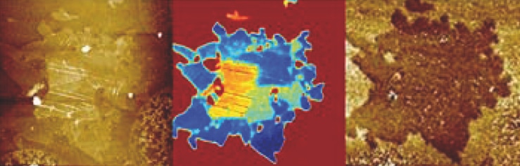
Figure 3 : Topgography (a), surface potential (b) and phase (c) channels of a graphene aggregate on SiO2 substrate showing flakes of 1, 2 and 3 layers
HD-KFM : HIGH ACCURACY AND SENSITIVITY TO DIFFERENT MATERIALS.
In order to test the accuracy of the surface potential values obtained with Bimodal HD-KFM, a standard sample test for KFM was imaged. This sample consists of a silicon substrate with two different metals (Gold and Aluminum) regions of 100 nm height defined by lithography. It is easy to find a region where three different materials are exposed (Gold-Silicon-Aluminum) thus, defining clear regions for the surface potential image. Figure 4 shows a 3D representation of this area with an overlapping of the of the corresponding surface potential image(different colors indicate different SP value). Every material can be clearly distinguished in the SP image with enough resolution as can be seen in the histogram of the colour-scale bar on the right side. Figure 5 shows both topography and SP images and a cross-section. It is important to notice that the SP cross-section (white line) shows no bending due to capacitive influences of tip and cantilever or averaging with the surrounding areas (Au and Al regions are 100 nm high). Even more, HD-KFM shows its high sensitivity as an intermediate region between silicon and Aluminum can be resolved. This region might be an effect of the lithography process or the fabrication of the sample as the topography reveals that the Aluminum area is not as flat as the gold area. The differences in the SP values between the Au-Si-Al areas are consistent with standard values of the work function for each material.
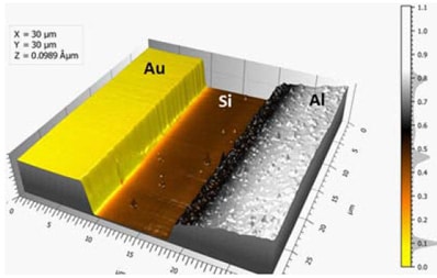
Figure 4 : 3D view with colour overlay of surface potential values of a kfm test sample with well-defined Au-Si-Al regions measured in ambient conditions.
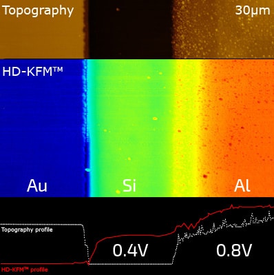
Figure 5 : Topography (top), surface potential (middle) and cross-section (bottom) of molibdene disulfide on gold substrate. High sensitivity of bimodal HD-KFM reveals a transition region between silicon and aluminum. Values are in good agreement with the bulk values of work functions.
技術規格
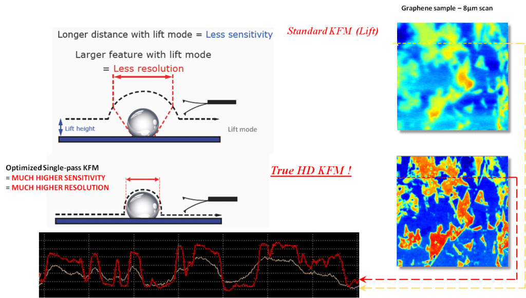
Single pass VS dual pass (lift)---- "Much higher sensitivity and resolution "
One of the clear advantages of the single pass approach as compared to the double pass implementation is the enhancement of resolution and sensitivity as the tip remains in the noncontact regime, but also much closer to the surface as illustrated in the figure below. A direct comparison between both techniques is made on a graphene sample over a SiC substrate. The contact potential image obtained in single-pass setup provides better contrast and lateral resolution of the graphene domains. This is due to the fact that in a single pass approach, the tip is oscillating closer to the surface (typically 0.1 nm-0.3 nm or touching the surface intermittently) as compared to the doublepass mode or lift mode (typically 10 nm-20 nm). As the electric field decays with the separation distance, standard double-pass has an intrinsic loss of sensitivity and lateral resolution.
如對此AFM有何技術上之問題或委測需求,歡迎來電: 02-2793-3133 或MAIL至 david.chang@utekmaterial.com
我們將為您提供最即時的諮詢與技術服務。